- 您现在的位置:买卖IC网 > Sheet目录1223 > KIT10XS3535EVBE (Freescale Semiconductor)KIT EVAL BOARD FOR 10XS3535
�� �
�
�FUNCTIONAL� DEVICE� OPERATION�
�LOGIC� COMMANDS� AND� REGISTERS�
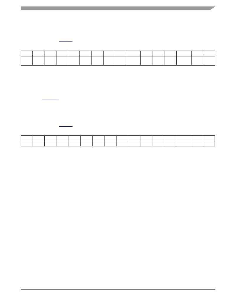
�PREVIOUS� ADDRESS� SOA[1:0]� =� 10�
�If� the� previous� two� LSBs� are� 10,� bits� OD15� :� OD0� reflect� the�
�status� of� the� 10XS3535� (� Table� 14� ).�
�Table� 14.� Device� Status�
�OD15�
�OD14�
�OD13�
�OD12�
�OD11�
�OD10�
�OD9�
�OD8�
�OD7�
�OD6�
�OD5�
�OD4�
�OD3�
�OD2�
�OD1�
�OD0�
�1�
�0�
�UVF�
�OTW�
�OTS�
�NM�
�0�
�OV�
�FOG_� IGN_ON� FLASH�
�RC�
�FOG� pin� FLASHER� IGN� pin� CLOCK�
�ON�
�ER_ON�
�pin�
�fail�
�OD13� (UVF)� =� Under-voltage� Flag� on� Vbat�
�OD12� (OTW)� =� Over-temperature� Prewarning� Flag�
�OD11� (OTS)� =� Over-temperature� Flag� for� all� outputs�
�OD10� (NM)� =� Normal� mode�
�OD8� (Overvoltage)� =� Over-voltage� Flag� on� Vbat� in� real� time�
�OD7� =� Indicates� the� state� of� internal� FOG_ON� signal� ,� as�
�described� in� Figures 11�
�OD6� =� Indicates� the� state� of� internal� IGN_ON� signal�
�OD5� =� Indicates� the� state� of� internal� FLASHER_ON� signal�
�OD4� (RC)� =� Logic� [0]� indicates� a� Front� Penta� Device.� Logic� [1]� indicates�
�a� Rear� Penta� Device�
�OD3� (FOG� pin)� =� indicates� the� FOG� pin� state� in� real� time�
�OD2� (FLASHER� pin)� =� Indicates� the� FLASHER� pin� state� in� real� time�
�OD1� (IGN� pin)� =� Indicates� the� IGN� pin� state� in� real� time�
�OD0� (CLOCK� fail)� =� Logic� [1],� which� indicates� a� clock� failure.� The�
�content� of� this� bit� is� reset� by� read� operation.�
�PREVIOUS� ADDRESS� SOA[1:0]� =� 11�
�If� the� previous� two� LSBs� are� 11,� bits� OD15� :� OD0� reflect� the�
�status� of� the� 10XS3535� (� Table� 15� ).�
�Table� 15.� Output� Status�
�OD15�
�1�
�OD14�
�1�
�OD13�
�UVF�
�OD12�
�OTW�
�OD11�
�OTS�
�OD10�
�NM�
�OD9�
�0�
�OD8�
�0�
�OD7�
�X�
�OD6�
�X�
�OD5�
�X�
�OD4�
�OUT5�
�OD3�
�OUT4�
�OD2�
�OUT3�
�OD1�
�OUT2�
�OD0�
�OUT1�
�OD13� (UVF)� =� Under-voltage� Flag� on� Vbat�
�OD12� (OTW)� =� Over-temperature� Prewarning� Flag�
�OD11� (OTS)� =� Over-temperature� Flag� for� all� outputs�
�OD10� (NM)� =� Normal� mode�
�OD4� (OUT5)� =� Logic� [0]� indicates� the� OUT5� voltage� is� lower� than�
�V� OUT_TH� .� Logic� [1]� indicates� the� OUT5� voltage� is� higher� than�
�V� OUT_TH�
�OD3� (OUT4)� =� Logic� [0]� indicates� the� OUT4� voltage� is� lower� than�
�V� OUT_TH� .� Logic� [1]� indicates� the� OUT4� voltage� is� higher� than� V� OUT_TH�
�OD2� (OUT3)� =� Logic� [0]� indicates� the� OUT3� voltage� is� lower� than�
�V� OUT_TH� .� Logic� [1]� indicates� the� OUT3� voltage� is� higher� than� V� OUT_TH�
�OD1� (OUT2)� =� Logic� [0]� indicates� the� OUT2� voltage� is� lower� than�
�V� OUT_TH� .� Logic� [1]� indicates� the� OUT2� voltage� is� higher� than� V� OUT_TH�
�OD0� (OUT1)� =� Logic� [0]� indicates� the� OUT5� voltage� is� lower� than�
�V� OUT_TH� .� Logic� [1]� indicates� the� OUT1� voltage� is� higher� than� V� OUT_TH�
�MC10XS3535�
�Analog� Integrated� Circuit� Device� Data� ?�
�Freescale� Semiconductor�
�33�
�发布紧急采购,3分钟左右您将得到回复。
相关PDF资料
KIT13892VLEVBEJ
KIT EVAL FOR MC13892
KIT17C724EPEVBE
KIT FOR 17C7242CH HBRIDGE PWR IC
KIT33810EKEVME
BOARD EVAL FOR MC33810
KIT33811EGEVBE
KIT EVAL 33811 SOLENOID MON IC
KIT33812ECUEVME
KIT DESIGN FOR 33812/S12P
KIT33812EKEVBE
BOARD EVALUATION FOR MC33812
KIT33879AEKEVBE
BOARD EVALUATION FOR MC33879
KIT33880DWBEVB
KIT EVAL FOR MC33880 8X SW W/SPI
相关代理商/技术参数
KIT10XS4200EVBE
制造商:Freescale Semiconductor 功能描述:EVAL BOARD, MC10XS4200 HIGH SIDE SWITCH; Silicon Manufacturer:Freescale; Silicon Core Number:MC10XS4200; Kit Application Type:High Side Switch; Application Sub Type:-; Kit Contents:Eval Board MC10XS4200, CD ROM
KIT-1113C
制造商:ABIKO 功能描述:Bulk
KIT1116-400
制造商:Laird Technologies Inc 功能描述:ANTKIT,FG 128-137MHZ/ODB + FM2
KIT-113-175C
制造商:LG Corporation 功能描述:KIT TUNER 113-175C (113-175E +
KIT1133-P250
功能描述:ANTKIT GB8W15FT CABLE 制造商:laird technologies ias 系列:* 零件状态:在售 标准包装:1
KIT-11591
功能描述:ISP POGO ADAPTER KIT 制造商:sparkfun electronics 系列:- 零件状态:在售 套件类型:初级入门套件 主要用途:ISP Pogo 适配器 标准包装:1
KIT1167-120
制造商:Laird Technologies Inc 功能描述:ANT KIT GPS1575PW 20FT 制造商:Laird Technologies Inc 功能描述:ANTKIT,GPS1575PW/20FT
KIT1185-120
制造商:Laird Technologies Inc 功能描述:KIT ANT GPS 20FT 制造商:Laird Technologies Inc 功能描述:KIT1185-120